Friday’s Lesson: How Transistors Work
Microelectronics is a subfield of electronics that studies very small electronic components, circuits, and systems. The foundation of information technology, microelectronics is also central to the current nanotechnology revolution. Many recent innovations, such as system-on-a-chip, microelectromechanical systems, gene chips, and lab-on-a-chip are either a direct outgrowth of microelectronics or a blend of it with other disciplines.
Although technology and engineering courses at the high school and college level now include microelectronics, teaching this subject is no small matter! The pedagogical challenge arises because microelectronics is a synthesis of many high-level fields, including solid-state physics, quantum mechanics, thermodynamics, statistical mechanics, electronics, and signal processing. Most curriculum materials employ mathematical formulation and didactic instructions. While this approach may work for advanced college students, the learning curve is far too steep for most high school and community college students.
The NSF-funded Electron Technologies project is exploring novel ways to make microelectronics more accessible to a wider audience. Our strategy utilizes computational modeling and visualization of electron dynamics in micro systems. If seeing is believing, we hope seeing is also understanding as the invisible world of electrons becomes visible and dynamic.
In this lesson, we present an activity for teaching transistors, which was created using our Molecular Workbench software.
The importance of transistors
Transistors are the building blocks of digital electronic devices. Your cell phone, MP3 player, and computer all depend on them to operate. Transistors can be made very tiny and massively produced using advanced microfabrication technology. You are probably using millions of them if you are reading the electronic version of this article—as of 2008, an Intel microprocessor contained nearly 2 billion transistors.
Exploring the field effect
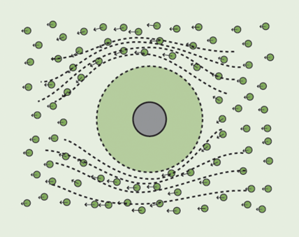
In a physics course, students may have learned: 1) electric fields cause the flow of electrons and 2) changing electric charges can affect the distribution of electric fields. Few students, however, understand that electric fields not only drive but also obstruct electric currents. The first model (Figure 1) in the activity is designed to show these field effects.
The model shows the flow of electrons, represented by the small circles with arrows that indicate their velocities around a negatively charged “island,” represented by the large gray circle in the middle. Students can change the total charge on the island and observe how it affects the flow of the electrons. Due to the Coulombic repulsions between the electrons and the island, there is an area around the island which the electrons are prohibited from entering. This forbidden area is shown as a green circle with a dashed outline.


Before manipulating the model, consider the following questions:
- What would happen to the forbidden area if the amount of charge on the “island” increases or decreases?
- What would happen if the island moves to a different location?
The size of the forbidden area determines the extent of constriction and, therefore, where the electric current can flow.
Experimenting with the junction field effect transistor
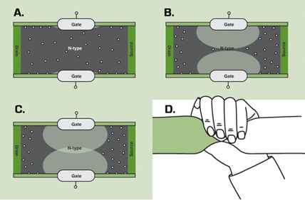
Having obtained a concrete picture about the field effect, students explore how this effect can be used to turn an electric current on and off like a switch in a junction field effect transistor (JFET) (Figure 2).
A JFET consists of a bulk semiconductor that provides the charge carriers, a source from which electrons flow in, a drain through which electrons flow out, and two gates that control the current flowing from the source to the drain. A voltage can be applied between a gate and the source to generate the field effect. When there is no voltage or the voltage is low, the electrons flow through the bulk semiconductor. When the voltage increases, the flow can be impeded. When the voltage reaches a certain value, the flow is completely pinched off. Like a garden hose, which you can squeeze to slow or stop the water flow, a JFET uses an electric field to achieve a similar effect.
Building logic gates
In the rest of the activity, students explore an AND gate and an OR gate built from two JFETs, thus understanding how transistors can be used to build integrated circuits (chips).
From microelectronics to nanoelectronics
The smaller a single transistor can be made, the more we can build into a chip and the faster it will compute. The last four decades have witnessed the reign of Moore’s Law in the computer industry, which states that the number of transistors on a chip doubles approximately every two years. The trend is not expected to stop for at least another decade, thanks to the advent of nanoelectronics.
When transistors become as small as a few nanometers, we enter the realm of nanotechnology. Sciences are rapidly converging, blending, and unifying in this fertile field, which may well be the main locomotive for the next Industrial Revolution. Today’s high school and college teachers must prepare students for future nanotechnician jobs.
